
5G Wireless Modules Enabled by Additive Manufacturing Technologies
Tong-Hong Lin, Jimmy G.D. Hester, Aline Eid, and Manos M. Tentzeris, Georgia Institute of Technology
This email address is being protected from spambots. You need JavaScript enabled to view it.
IEEE Future Networks Tech Focus, Volume 3, Number 1, March 2019
Abstract
Additive manufacturing technologies, including inkjet and 3D printing, display remarkable features that enable new and creative solutions to the challenges faced by 5G wireless systems. Their materials versatility and ability to seamlessly accommodate complex geometries open new opportunities in the areas of 5G-compatible mm-wave packaging and flexible, durable, and wearable 5G-enabled IoT systems. Their low tooling costs and rapid iteration capabilities also stand out in view of their use for large-scale quick-to-market fabrication of complex 5G devices, systems, and products. Here the authors demonstrate these capabilities by presenting examples of outstanding high-performance mm-wave 5G packaging, long-range RFID sensing systems, and wearable energy harvesters fabricated using low-cost additive manufacturing approaches.
1. Introduction
5G protocols and approaches have been introduced to accommodate the growing demand for high-speed data transmission and service. This can only be achieved through the use of higher bandwidths and frequencies, both of which requiring a rise to mm-wave frequency operation, which induce new challenges as well as new potentials. For starters, the larger parasitics suffered at mm-wave frequencies can have serious impacts on the performance of carelessly packaged ICs. Moreover, due to the high path loss incurred in these bands and to the low sensitivities of the 5G-required wide-band receivers, much more intricate and complex antenna array systems with high gains are required to conserve practical communication ranges. Despite these challenges, and in addition to its remarkable communications capabilities, 5G bands allow a significant shrinking of the sizes of RF components that is perfect for the introduction of new system on package (SoP) designs and miniaturized wearable electronic systems.
Additive manufacturing techniques such as inkjet printing and 3D printing have been proposed to overcome the new challenges posed by 5G operation. Additive manufacturing techniques are low cost, fast prototyping techniques with high resolution (around 20 µm), making them suitable for applications at 5G and mm-wave range. They support a very high level of material versatility, by enabling the use of flexible, wearable, and durable conductive, semiconducting, reactive (i.e. sensing), and dielectric materials, so that entire systems can be printed from the ground up. Finally, the 3D structural flexibility allows major size reductions and intricate full-3D SoP designs.
This article introduces several examples of 5G designs and applications utilizing additive manufacturing techniques to solve the aforementioned challenges and explore their potential. Section 2 introduces a SoP design with an integrated packaged broadband antenna. The additively-manufactured ramps are used to replace the inter-layer interconnects, which offer much smaller parasitics than conventional processes. In section 3, printed gas-sensing Van-Atta arrays, backscatter topologies capable of overcoming path-loss-related challenges and enabling long-range and energy autonomous 5G-enabled ubiquitous IoT constellations are presented. Finally, in section 4, flexible and wearable energy harvesters capable of powering this new generation of 5G IoT devices are introduced.
2. 5G System on Package (SoP) Modules
|
(a) |
(b) |
|
 (c)
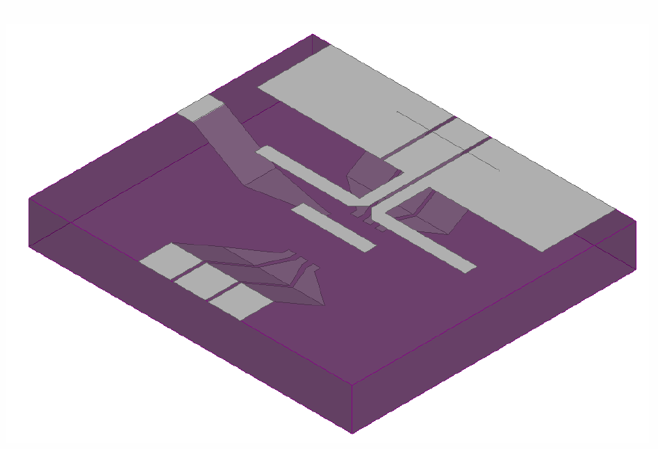
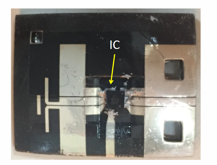
(c) Figure 1(a): 3D and inkjet printed mm-wave SoP design (b) SoP design with IC attached and (c) miniaturized 3D and inkjet printed SoP design. [1]
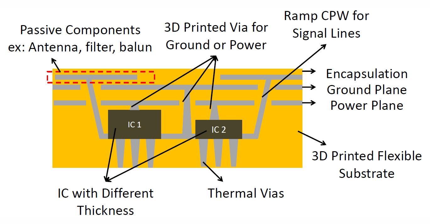
The small wavelengths at 5G frequencies make the size of RF components small enough to be integrated into the package, and thus lead to numerous package integrated designs [1]-[2]. SoP topologies which integrated the integrated circuits (ICs) with peripheral components such as filters, couplers, and antennas then became one of the most popular 5G applications. However, there are couple of challenges needed to be addressed. First, as we move to the 5G frequencies, the high parasitics from packaging such as wire-bonds and interconnections start to have huge effects on the IC performance. Second, since the high data transmission rate is the result of broader bandwidth, a broadband antenna design and a simple way to integrate it with the package are necessary. Finally, in order to apply the SoP module to broader applications such as wearable electronics, the substrate and package structure have to be able to resist the shocks and vibrations due to human movement.
In order to solve the new challenges as well as realize the SoP designs, a new fabrication process and packaging design are crucial. Additive manufacturing techniques including inkjet printing and 3D printing are proposed and used to deposit both the substrates and conductors. In [1], we introduce an additively manufactured 5G module with low-parasitic flexible packaging. With the high flexibility in the structures and materials, 3D and complex SoP design as shown in Figure 1(a) can be achieved. As shown in Figure 1(a), the substrates can be fabricated layer by layer using 3D printing techniques. The conventional thermal vias and vias for ground and power plane can be fabricated by 3D printed via holes and filled with silver ink. However, via connections are not suitable for 5G and mm-wave signal transmission because of their high parasitics. On the other hand, 3D printed ramp structure and inkjet printed silver CPW traces on the ramp to form die-to-substrate and inter-layer connections are suitable since they are transmission lines and will induce much smaller parasitic compared with conventional approaches [1],[3].
A broadband Yagi antenna covering the entire 5G band from 24.5 GHz to 29.5 GHz is proposed and fabricated using 3D and inkjet printing. The ability of realizing complex 3D structure makes it easy to be integrated with the package as Figure 1(b) demonstrated. The overall size is reduced by placing the antenna right on the top of the IC. The 3D printed flexible resin, FLGR02, is used as the flexible substrate so that the packaging has better resist to vibrations and shocks. Thus, the proposed 5G module is suitable for wearable platform where constant human movements are involved. The fabrication process including solutions to surface treatment for ink adhesion, smooth of surface roughness, and CTE mismatch between the flexible material and the silver ink are proposed. The wireless module, as shown in Figure 1(c), including a broadband Yagi antenna which covers the entire 5G band located at 24.5 GHz – 29.5 GHz and a LNA IC are fabricated. The size can be further reduced to Figure 1(b) by excluding the space for SMA connectors and folding the antenna to the top of the IC.
3. 5G and mm-wave RFIDs Using Van-Atta Arrays
|
|
|
|
 (a)
(a)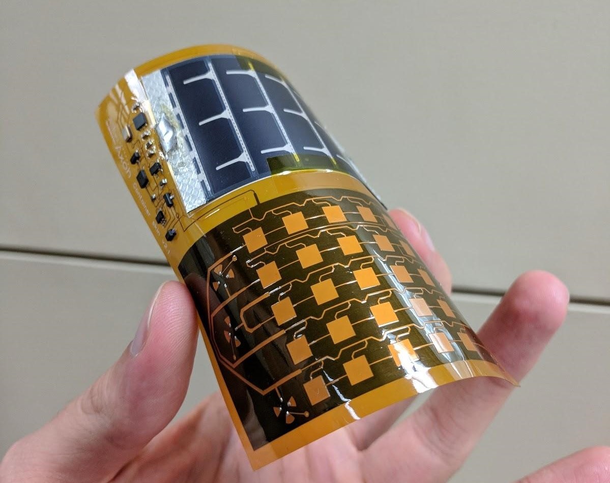 (b)
(b)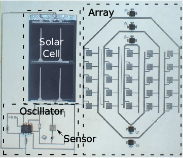 (c)
(c)Figure 2(a): Ultra-long-range interrogation of a chipless chipless tag, (b) 5G IoT Smart-Skin tag, and (c) additively-manufactured tag with a printed Carbon NanoTubes-based ammonia sensor [6,7]
Most of the interest into 5G wireless communication networks has, understandably, been focused upon the prospect of their ability to offer blazingly-fast and ultra-low-latency service in densely-populated urban contexts. Nevertheless, part of the unique technological artillery deployed for the implementation of the 5G project can be used for the benefit of alternative applications. One of these newly-accessible fields is that of mm-wave RFIDs.
Path loss is a recurring metric used to assess the relative maximum range of communication channels, according to their frequency of operation. Its square dependency on frequency (higher frequency, higher loss) is often mentioned to predict or justify a range penalty incurred by systems operating at mm-wave frequencies. Nevertheless, the frequency dependency of this law does not result from the fundamental properties of electromagnetic propagation, but rather from the shrinking size of equal-gain antennas at higher frequencies. In other terms, high-frequency path loss is not a first-principles, fundamentally-limiting, unmovable obstacle: it is, at its core, an antenna engineering problem.
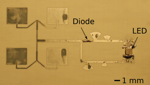
The ATHENA group at Georgia Tech has demonstrated that a set of unique features, including greatly extended reading ranges, can be achieved by RFIDs functioning at mm-wave frequencies, more than one order of magnitude higher than the operation of current commercial backscatter UHF devices. This feat arises from the use of electrically-large retrodirective antenna front-ends, such as Van-Atta reflect-arrays, which can deliver a high equivalent gain in a semi-isotropic fashion. This insight was first applied to the design of a chipless RFID reported in [4] and expanded in [5], [6]. The tag, a fully-inkjet-printed humidity-sensing cross-polarizing Van-Atta reflectarray operating in the Ka-band, achieved a reading range in excess of 30m [2], an order-of-magnitude higher than the state of the art of chipless RFIDs, which was then extended to 58 m, as shown in Figure 2(b) [6]. A semi-passive backscatter-communications-enabled version of a similar antenna system, shown in Figures 2(b) and 2(c), was then used to report the longest-ranging RFID, with a range of 80 m [7]. The tag, with its energy-autonomous ultra-low-power continuous transmissions, was enabled with real-time ammonia sensing capabilities, thereby making it a perfect solution for real-time ubiquitous gas monitoring applications.
4. Flexible and Wearable Energy Harvesters
|
|
|
 (a)
(a) 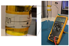 (b)
(b) Figure 3 (a): Flexible 24 GHz rectenna prototype on LCP substrate, (b) Flexible 2.4 GHz rectenna measurement on the 0.75” radius cylinder [8,9]
RF energy harvesting networks have been drawing significant attention because of their potential to power millions of autonomous devices and wearable electronics using ambient RF and mm-wave energy [8]-[11]. It has been proposed as the main energy source for low power consumption and low duty cycle devices. Schottky diodes have been and still are the components of choice for rectifiers in many of the wireless energy harvesting systems because of their inherently low turn-on voltage, which provides high efficiency, as well as their technological maturity. The new 5G bands are allowed to use much higher Equivalent Isotropically Radiated Power (EIRP) than their lower frequency counterpart, which makes them very attractive and a potential source of harvested power. However, one of the main challenges of ambient mm-wave energy harvesting is the requirement for diodes to operate at frequencies, in and beyond the Ka band. Recently, one effort has indicated the potential of Schottky diodes for mm-wave energy harvesting rectifiers. The proposed design in [8] has demonstrated a flexible, inkjet-printed 24 GHz rectenna as shown in Figure 3(a). The antenna array has shown a realized gain of 5 dBi, printed along with a single-lumped-component via-less rectifier with up to a 2.5 V dc voltage for an input power of 18 dBm, at the operation frequency of 24 GHz.
One of the most enticing applications of these circuits is their use to power wearable devices, which require a unique combination of properties such as compactness, high efficiency, flexibility and stability relative to bending. A printed system, presented in [9], demonstrated all of these features in a wireless operation test, in a bent condition, thereby setting the foundation for the emergence of mm-wave powered smart skins and wearables for the Internet of Things. In this paper, a compact ultra-lightweight RF energy harvester is presented, it is fabricated on a 0.18 mm thick liquid crystal polymer (LCP) flexible substrate (dielectric constant of 3) using an inkjet-printed masking technique followed by etching. The proposed rectenna is designed to operate over the 2.4 GHz ISM band, however a different diode instead of the SMS7630 with higher cut-off frequency such as the MA4E2038 model from Macom can be used to tune the frequency operation of this rectifier towards 5G applications. The rectifier includes a dual transmission lines tapered matching network that provides a combination of compactness, flexibility and an efficiency of up to 40%. A miniaturized monopole antenna is integrated with the aforementioned rectifier forming an ultra-compact, efficient and flexible rectenna as shown in Figure 3(b). The system has demonstrated very stable performance when characterized in multiple bent, displaying a variation in harvested power that is less than 57 % while placed over a planar surface as well as curvatures such as cylinders of 0.75”, 1.5” and 2” radii.
These promising results of flexibility and robustness prove the large potential of mm-wave energy harvesters in leading the new world of 5G-powered applications.
5. Conclusion
In this article, integrated additively manufactured 5G packaging and broadband SoP modules offering 10 times smaller parasitic compared with conventional packaging techniques, printed mm-wave tags with more than 10 times the range of the previous state of the art, and ultra-compact energy harvesters were demonstrated. Additively manufactured 5G devices and systems, despite these impressive results, remain in their infancy and are yet to reveal the extent of their potential. Their use promises the advent of rapidly-reconfigurable mass-produced 5G SoP modules, and the birth of dense implementations of energy-autonomous smart skins to enable reliable, and maintenance-free ubiquitous intelligence and sensing.
References
- T.-H. Lin, R. Bahr, M. Tentzeris, R. Pulugurtha, V. Sundaram and R. Tummala, "Novel 3D-/Inkjet-Printed Flexible On-package Antennas, Packaging Structures, and Modules for Broadband 5G Applications," 2018 IEEE 68th Electronic Components and Technology Conference (ECTC), San Diego, CA, 2018, pp. 214-220.
- T.-H. Lin, P. M. Raj, A. Watanabe, V. Sundaram, R. Tummala and M. M. Tentzeris, "Nanostructured miniaturized artificial magnetic conductors (AMC) for high-performance antennas in 5G, IoT, and smart skin applications," 2017 IEEE 17th International Conference on Nanotechnology (IEEE-NANO), Pittsburgh, PA, 2017, pp. 911-915.
- K. Tehrani, R. A. Bahr, W. Su, B. S. Cook, and M. M. Tentzeris, “E-band characterization of 3d-printed dielectrics for fully-printed millimeter-wave wireless system packaging,” in 2017 IEEE MTT-S International Microwave Symposium (IMS), June 2017, pp. 1756–1759.
- G. D. Hester and M. M. Tentzeris, "Inkjet-printed Van-Atta reflectarray sensors: A new paradigm for long-range chipless low cost ubiquitous Smart Skin sensors of the Internet of Things," 2016 IEEE MTT-S International Microwave Symposium (IMS), San Francisco, CA, 2016, pp. 1-4.
- G. D. Hester and M. M. Tentzeris, "Inkjet-Printed Flexible mm-Wave Van-Atta Reflectarrays: A Solution for Ultralong-Range Dense Multitag and Multisensing Chipless RFID Implementations for IoT Smart Skins," in IEEE Transactions on Microwave Theory and Techniques, vol. 64, no. 12, pp. 4763-4773, Dec. 2016.
- Henry, J. G. D. Hester, H. Aubert, P. Pons and M. M. Tentzeris, "Long-Range Wireless Interrogation of Passive Humidity Sensors Using Van-Atta Cross-Polarization Effect and Different Beam Scanning Techniques," in IEEE Transactions on Microwave Theory and Techniques, vol. 65, no. 12, pp. 5345-5354, Dec. 2017.
- G. D. Hester and M. M. Tentzeris, "A Mm-wave ultra-long-range energy-autonomous printed RFID-enabled van-atta wireless sensor: At the crossroads of 5G and IoT," 2017 IEEE MTT-S International Microwave Symposium (IMS), Honololu, HI, 2017, pp. 1557-1560.
- Bito et al., "Millimeter-wave ink-jet printed RF energy harvester for next generation flexible electronics," 2017 IEEE Wireless Power Transfer Conference (WPTC), Taipei, 2017, pp. 1-4.
- Eid, Aline et al.” A Flexible Compact Rectenna for 2.4GHz ISM Energy Harvesting Applications.” International Symposium on Antennas and Propagation and USNC-URSI Radio Science Meeting (APS/USRI), IEEE, 2018.
- T.-H. Lin et al., "On-Body Long-Range Wireless Backscattering Sensing System Using Inkjet-/3-D-Printed Flexible Ambient RF Energy Harvesters Capable of Simultaneous DC and Harmonics Generation," in IEEE Transactions on Microwave Theory and Techniques, vol. 65, no. 12, pp. 5389-5400, Dec. 2017.
- T.-H. Lin, W. Su and M. M. Tentzeris, "Expand Horizons of Microfluidic Systems: An Inkjet Printed Flexible Energy Autonomous Micropump System for Wearable and IoT Microfluidic Applications," 2018 IEEE/MTT-S International Microwave Symposium - IMS, Philadelphia, PA, 2018, pp. 812-815.
 Tong-Hong Lin (S’18) received the B.S.E.E. and M.S. degree from National Taiwan University, Taipei, Taiwan, R.O.C, in 2011 and 2013. He is currently working toward the Ph.D. degree in electrical and computer engineering at Georgia Institute of Technology, Atlanta, GA, USA. He is now a Research Assistance in ATHENA group. His current research interests include applying additive manufacturing such as inkjet printing and 3D printing to wearable and flexible electronics, RF energy harvesting systems, wireless power transfer systems, and wireless sensing networks. He is the winner of 2018 Electronic Components and Technology Conference (ECTC) Student Travel Award.
 Jimmy G.D. Hester (S’14) spent two preparation years in fundamental chemistry, math and physics after which he was admitted in INP Toulouse, ENSEEIHT where he received a graduate degree and M.S degree in electrical and signal processing engineering, majoring in radio frequency electronics, in 2012 and 2014, respectively. He received the M.S. in electrical and computer engineering from the Georgia Institute of Technology, Atlanta, in 2014 where he is now working, as a research assistant in the ATHENA group, towards his PhD degree in Electrical and Computer Engineering. His research interests lie at the interface between radio frequency and mm-wave engineering and material science, in the form of flexible electronics technologies and nanotechnologies. Recently, he has been developing solutions for the use of carbon nanomaterials as well as optimized RF structures towards the implementation of inkjet-printed flexible low cost ubiquitous gas sensors for Internet of Things and Smart Skin applications. His work covers the entire development process, from the development of inkjet inks, improvement of fabrication methods, sensor component design, high frequency characterization and environmental testing to the design, simulation and fabrication of the RF system embedding the sensor, and the development of wireless reading and data processing schemes. He was awarded the 2015 NT4D Student Award, a 2nd place Best Poster Award at the 2017 IEEE Futurecar conference, a 3rd place Best Poster Award at the 2017 Flex conference, and a Honorable Mention Award as finalist of the 2017 IMS student paper competition.
 Aline Eid received her B.E. in Electrical Engineering from Notre Dame University, Louaize, Lebanon in 2015 and her masters in Electromagnetics, Antennas and RF Systems from the American University of Beirut, Lebanon, in 2017. She is currently a PhD student in Electrical and Computer Engineering at the Georgia Institute of Technology. Her work focuses on the simulation, design and fabrication of printed RF electronics, more specifically RF energy harvesting systems and fully printed active devices.
 Manos M. Tentzeris (S’89–M’92–SM’03–F’10) received the Diploma Degree in Electrical and Computer Engineering from the National Technical University of Athens ("Magna Cum Laude") in Greece and the M.S. and Ph.D. degrees in Electrical Engineering and Computer Science from the University of Michigan, Ann Arbor, MI and he is currently Ken Byers Professor in Flexible Electronics with School of ECE, Georgia Tech, Atlanta, GA. He has published more than 650 papers in refereed Journals and Conference Proceedings, 5 books and 25 book chapters. Dr. Tentzeris has helped develop academic programs in 3D/inkjet-printed RF electronics and modules, flexible electronics, origami and morphing electromagnetics, Highly Integrated/Multilayer Packaging for RF and Wireless Applications using ceramic and organic flexible materials, paper-based RFID's and sensors, wireless sensors and biosensors, wearable electronics, "Green" electronics, energy harvesting and wireless power transfer, nanotechnology applications in RF, Microwave MEM's, SOP-integrated (UWB, multiband, mmW, conformal) antennas and heads the ATHENA research group (20 researchers). He has served as the Head of the GT-ECE Electromagnetics Technical Interest Group, as the Georgia Electronic Design Center Associate Director for RFID/Sensors research and as the Georgia Tech NSF-Packaging Research Center Associate Director for RF Research and the RF Alliance Leader. He was the recipient/co-recipient of the 2017 Georgia Tech Outstanding Achievement in Research Program Development Award, 2016 Bell Labs Award Competition 3rd Prize, the 2015 IET Microwaves, Antennas and Propagation Premium Award, the 2014 Georgia Tech ECE Distinguished Faculty Achievement Award, the 2014 IEEE RFID-TA Best Student Paper Award, the 2013 IET Microwaves, Antennas and Propagation Premium Award, the 2012 FiDiPro Award in Finland, the iCMG Architecture Award of Excellence, the 2010 IEEE Antennas and Propagation Society Piergiorgio L. E. Uslenghi Letters Prize Paper Award, the 2011 International Workshop on Structural Health Monitoring Best Student Paper Award, the 2010 Georgia Tech Senior Faculty Outstanding Undergraduate Research Mentor Award, the 2009 IEEE Transactions on Components and Packaging Technologies Best Paper Award, the 2009 E.T.S.Walton Award from the Irish Science Foundation, the 2007 IEEE APS Symposium Best Student Paper Award, the 2007 IEEE IMS Third Best Student Paper Award, the 2007 ISAP 2007 Poster Presentation Award, the 2006 IEEE MTT Outstanding Young Engineer Award, the 2006 Asian-Pacific Microwave Conference Award, the 2004 IEEE Transactions on Advanced Packaging Commendable Paper Award, the 2003 NASA Godfrey "Art" Anzic Collaborative Distinguished Publication Award, the 2003 IBC International Educator of the Year Award, the 2003 IEEE CPMT Outstanding Young Engineer Award, the 2002 International Conference on Microwave and Millimeter-Wave Technology Best Paper Award (Beijing, CHINA), the 2002 Georgia Tech-ECE Outstanding Junior Faculty Award, the 2001 ACES Conference Best Paper Award and the 2000 NSF CAREER Award and the 1997 Best Paper Award of the International Hybrid Microelectronics and Packaging Society. He was the TPC Chair for IEEE IMS 2008 Symposium and the Chair of the 2005 IEEE CEM-TD Workshop and he is the Vice-Chair of the RF Technical Committee (TC16) of the IEEE CPMT Society. He is the founder and chair of the RFID Technical Committee (TC24) of the IEEE MTT Society and the Secretary/Treasurer of the IEEE C-RFID. He is the Associate
Editor of IEEE Transactions on Microwave Theory and Techniques, IEEE Transactions on Advanced Packaging and International Journal on Antennas and Propagation. Dr. Tentzeris was a Visiting Professor with the Technical University of Munich, Germany for the summer of 2002, a Visiting Professor with GTRI-Ireland in Athlone, Ireland for the summer of 2009 and a Visiting Professor with LAAS-CNRS in Toulouse, France for the summer of 2010. He has given more than 100 invited talks to various universities and companies all over the world. He is a Fellow of IEEE, a member of URSI-Commission D, a member of MTT-15 committee, an Associate Member of EuMA, a Fellow of the Electromagnetic Academy and a member of the Technical Chamber of Greece. Prof. Tentzeris served as one of the IEEE MTT-S Distinguished Microwave Lecturers from 2010-2012 and he is one of the IEEE CRFID Distinguished Lecturers.
Editor: Rod Waterhouse
Subscribe to Tech Focus
Join our IEEE Future Networks Technical Community and receive IEEE Future NetworksTech Focus delivered to your email.
Article Contributions Welcome
Submit Manuscript via Track Chair
Author guidelines can be found here.
Other Future Networks Publications
IEEE Future Networks Tech Focus Editorial Board
Rod Waterhouse, Editor-in-Chief
Mithun Mukherjee, Managing Editor
Imran Shafique Ansari
Anwer Al-Dulaimi
Stefano Buzzi
Yunlong Cai
Zhi Ning Chen
Panagiotis Demestichas
Ashutosh Dutta
Yang Hao
Gerry Hayes
Chih-Lin I
James Irvine
Meng Lu
Amine Maaref
Thas Nirmalathas
Sen Wang
Shugong Xu
Haijun Zhang
Glaucio Haroldo Silva de Carvalho